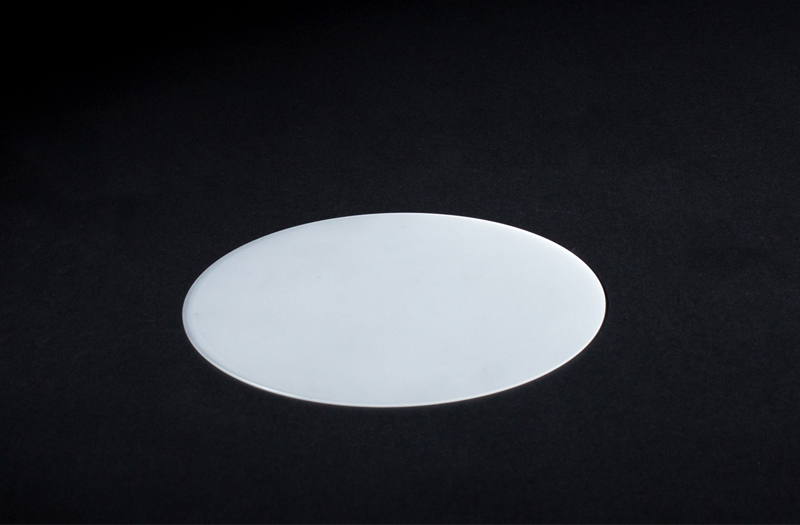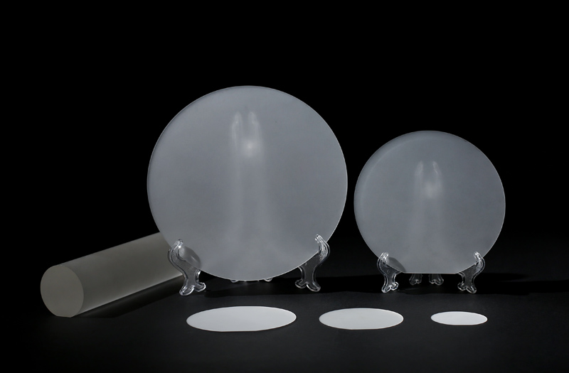
Due to the less mismatched lattice and stable chemical and physical properties, sapphire(Al2O3) wafer is the popular substrates for III-V nitrides, superconductor and magnetic epi-film. They are widely used in GaN and thin-film epitaxial growth, silicon on sapphire, LED market and optics industry.
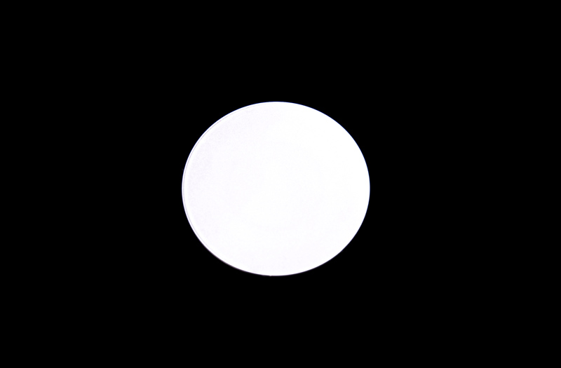
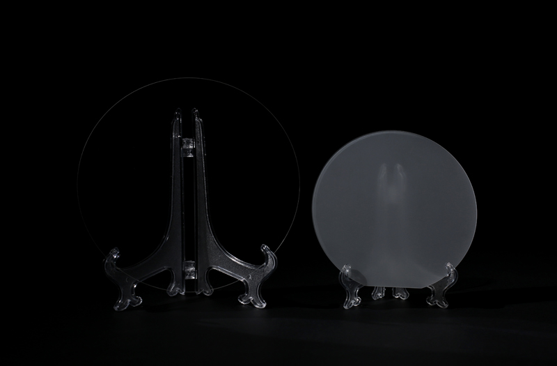
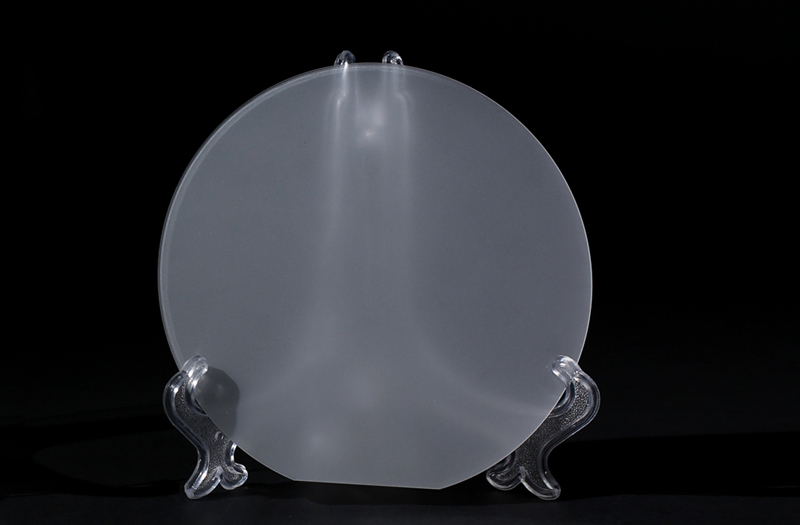
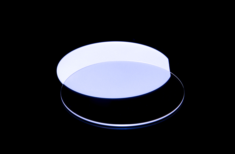
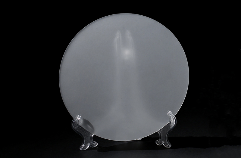
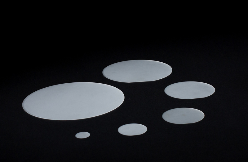
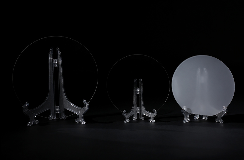
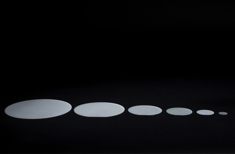
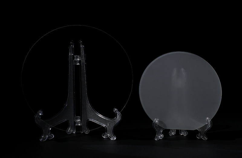
CRYSCORE is a professional sapphire wafer supplier who manufactures 99.999% high purity single crystal polished sapphire wafers for epitaxy. And our sapphire (Al2O3) substrates feature excellent surface finish, which is the key LED parameter.
If you are looking for reliable sapphire wafer suppliers, contact us now.
Among all China sapphire substrate suppliers, CRYSCORE has always devoted ourselves to the quality of sapphire substrates.
1. Sapphire has a high optical transmittance, so it is widely used as microelectronic tube dielectric material, ultrasonic conduction element, waveguide laser cavity, and other optical elements, as window materials for infrared military devices, space vehicles, high-intensity lasers and optical communications.
2. Sapphire has high rigidity, high strength, high working temperature, abrasion resistance, corrosion resistance characteristics, so sapphire substrate is often used in harsh environments, such as boiler water gauge (high-temperature resistance), commodity bar code scanner, bearing, and other precision manufacturing (wear resistance), coal, gas, well detection sensors and detector windows (anti-corrosion).
3. Sapphire has the characteristics of electrical insulation, transparency, good thermal conductivity, and high rigidity, so it can be used as the substrate material of integrated circuits, such as LED and microelectronic circuits, ultra-high-speed integrated circuit.
99.999 % high purity single crystal Al2O3 material.
Special CMP (Chemical Mechanical Polishing) technology to ensure the performance of Al2O3 substrate at a low cost.
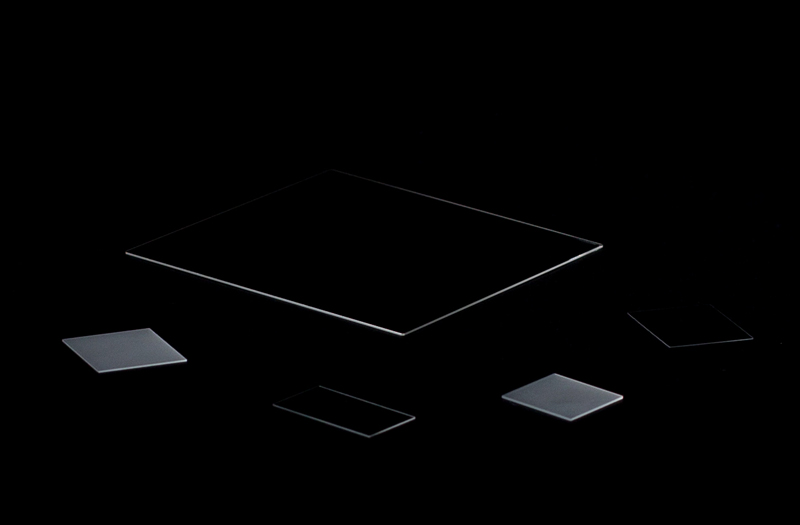
Excellent surface quality in all orientations (less than 0.2 nm for C-plane, less than 0.5 nm for A-plane, M-plane, R-plane, N-plane, V-plane, 10-14, etc.)
Cleaned in class 100 cleanroom by ultrapure water with quality above 18MΩ *cm.
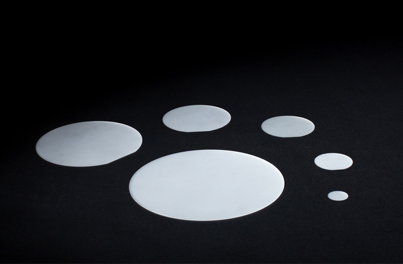
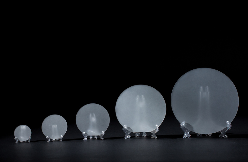
25 pcs a pack or single pack is available to maximize customer flexibility in their research.
Traceable product serial number.
Compact carton packaging for safer shipping and cost-saving.
Standard wafers are Generally in stock to ensure a quick delivery.
As one of best China sapphire wafer manufacturers, CRYSCOR is committed to supirior quality and cost-eefective sapphire substrates for your business.
CRYSCORE is one of sapphire ingot manufacturers, our unpolished or polished sapphire wafers are widely used in the industries of LED, semiconductor, microelectronic and more.
1. Semiconductor LED industry (MOCVD epitaxial GaN substrate)
In general, C-plane sapphire is needed in this area. R-plane or M-plane mainly used to grow non-polar/semi-polar plane epitaxial layers to improve the luminescence efficiency.
2. The growth of III-V or II-VI compound semiconductors.
3. Microelectronic IC applications especially Very High-Speed Integrated Circuit, SOS
Generally, it is a silicon heteroepitaxial deposition on R-plane sapphire.
4. Hybrid microelectronics
Hybrid microelectronics products are mainly HIC and MCM. It has high requirements on the substrate, while sapphire substrates' characteristics such as stable dielectric constant and low dielectric loss make sapphire wafer the most commonly used substrate for HIC and the main substrate for MCM. Generally, the A-plane sapphire wafer is needed.
At the very beginning, we have a crystal boule.
Crystal growing: Produce high-quality sapphire monocrystals via furnace.
Sapphire ingot processing: Drill out the ingot, Ground the ingot, Quality inspection.
Then we get the sapphire ingot.
Orientation: Position the ingot on the sawing machine.
Sawing: Cut the ingot into thin wafers.
Lapping: Lap the wafer to remove the scratched layer and improve its flatness.
Chamfer: Trim the edge of the wafer into an arc to improve the mechanical strength, to avoiding stress concentration.
Polishing: Reduce the surface roughness to reach the epitaxial wafer grade.
Cleaning: Remove dirt from the wafer surface.
Quality inspection: Inspect wafer with a high precision instrument to meet customer's requests.
Finally, we get the sapphire wafer.
Epitaxy wafer, or the so-called Epi wafer, is a kind of wafer that has gone through the process where a new single crystal layer had been added on a single crystal substrate. And normally, the newly added epi layer can be the same material as the substrate or it may be other materials according to different usage needs.
Epi wafer is a layer of semiconductor wafer deposited onto a wafer substrate. It involves the growth of crystals of one material on the crystal face of another (heteroepitaxy) or the same (homoepitaxy) material. The lattice structure and orientation or lattice symmetry of the thin film material are identical to that of the substrate on which it is deposited. The epitaxy wafer has better performance than the non-epi wafer in some fields, such as latch-up prevention in noisy environments (radiation hardening) as well as noise reduction and providing better matching of device biasing. But in terms of the pricing, the epi wafer is indeed more expensive. It has applications in nanotechnology and in the manufacture of semiconductor and photonic devices.

 Introduction to the Manufacturing Process of Sapphire Ingot
Company brochure
The Technical Difference Between the Kyropoulos Method and the Czochralski Method for Growing Sapphire Crystals
Introduction to the Manufacturing Process of Sapphire Ingot
Company brochure
The Technical Difference Between the Kyropoulos Method and the Czochralski Method for Growing Sapphire Crystals