
Sapphire wafer is the most widely used substrate material in semiconductor lighting industry, and patterned sapphire substrate (PSS) is the general method to improve the luminous efficiency of semiconductor lighting devices. These sapphire substrates are with periodic structures of various shapes such as cone, dome, pyramid, and pillar, etc.
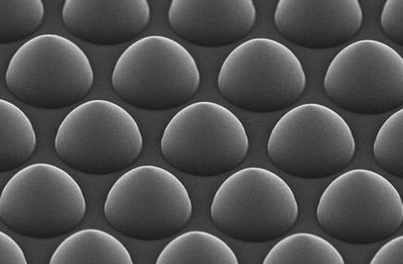
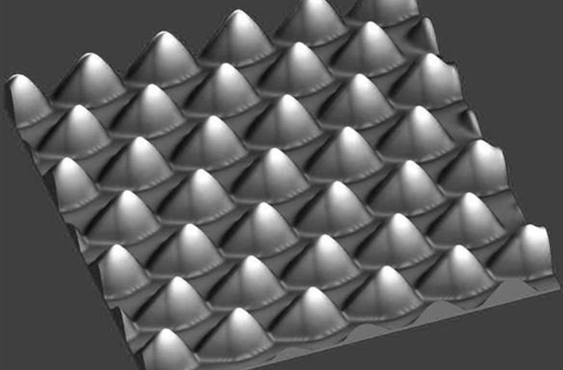
Pattern dimension, aspect ratio, and uniformity across the wafer as well as consistency from wafer to wafer, are important factors to improve the light extraction. Currently, we provide 2-inch and 4-inch patterned sapphire substrates (PSS sapphire and wafer) with the following specifications. Diameter: 2.7 +/- 0.1 μm. Spacing: 0.3 +/- 0.1 μm. Depth: 1.7 +/- 0.15 μm.

 Introduction to the Manufacturing Process of Sapphire Ingot
Company brochure
The Technical Difference Between the Kyropoulos Method and the Czochralski Method for Growing Sapphire Crystals
Introduction to the Manufacturing Process of Sapphire Ingot
Company brochure
The Technical Difference Between the Kyropoulos Method and the Czochralski Method for Growing Sapphire Crystals